
Dr. Akshay K.
Assistant Professor
- Room No: A-007, SECS
- +91 674713-5784
- akshay@iitbbs.ac.in
- School of Electrical and Computer Sciences
PRESS RELEASE & HIGHLIGHTS
Arsensafe developed by Nano Semic featured in The Hindu ! : Click here for more information
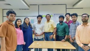
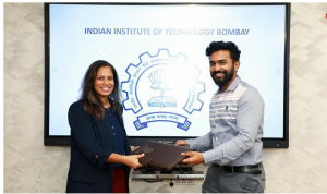
iVP Semi partners with IIT Bhubaneswar and IIT Bombay for developing next generation Silicon MOSFETs for eV applications : Click here for more information
IIT Bhubaneswar leading the efforts in setting up an industry co-development center on power devices for next generation research and manpower training. Click here for more information
Silicon Carbide Charge Sheet SuperJunction (CSSJ) featured as a promising power device in IITM Techtalk magazine. Click here for more information
- Research
- Biosketch
- Projects
- Teaching
- Mentoring
- Publication International
- Conference International
- Conference National
- Books & Patents
- Education
- Experience
- Awards
- Others
Dr. Akshay K. received a B.Tech degree in Electronics and Communication Engineering from NIT Calicut, in 2017 and an accelerated Ph.D. with M.S. in Electrical Engineering from IIT Madras in 2022 with Prime Minister’s Research Fellowship. His research interest is primarily on the design, and development of power semiconductor devices based on silicon and wide/ultra-wide bandgap semiconductors. He is the recipient of the Institute Research Award issued by IIT Madras and AWSAR Award issued by DST, Govt. of India. Prior to joining IIT Bhubaneswar he was a Senior Semiconductor Device Engineer in the Technology Development Group at Micron Technology Inc., where he was involved in the design and optimization of biasing schemes for next-generation non-volatile 3D-NAND flash memory transistor arrays.
At IIT Bhubaneswar, he leads the D-MOS research group with 4 PhD scholars and several masters and bachelors students. The research group has TCAD based process design and advanced characterization capability of power semiconductor devices and sensors and actively engages with leading power semiconductor companies for their research and development requirements. He is also a co-founder and Director of Nano Semic, a semiconductor products and services based startup registered with IIT BBS research park.
| Funding agency | Budget in lakhs (INR) | Start Date | End Date | Title | PI/Co-PI |
| iVP Semi (consultancy) | $ 100K USD | Apr 2025 | Apr 2027 | Design and Development of Si MOSFETs for eV application | PI |
| ANRF | 72 | March 2025 | March 2028 | Design and Characterization of SiC Trench MOSFETs for Next Generation Power Electronic Applications | PI |
| IIT Bhubaneswar | 20 | Oct 2025 | Oct 2027 | Simulation, Design and Feasibility Investigation of Superjunction based Power Devices in 4H-SiC Material | PI |
| INUP-i2i
(@IIT Bombay NF) |
in-kind support | Oct 2024 | Oct 2025 | Investigation of Al2O3/SiO2 Interface on Silicon Carbide Substrate to study the feasibility of Charge Sheet Super Junction | PI |
New Courses Introduced in Curriculum @ IIT Bhubaneswar
- Fundamentals of Semiconductor Devices: UG level
- Introduction to EDA Tools: UG level
- Power Semiconductor Devices and Technology: PG level
- MOS Device Modeling and Characterization: PG level
- Advanced Memory Devices: PG level
Theory and Lab Courses Handled @ IIT Bhubaneswar
- Power Semiconductor Devices and Technology to M.Tech and PhD.
- For B.Tech in ECE
- Fundamentals of Semiconductor Devices (1st year), Introduction to EDA Tools (2nd year), Introduction to Electronics (2nd year), VLSI Design: Theory and Lab courses (3rd year), Microprocessors and Microcontrollers: Theory and Lab courses (3rd year)
- For B.Tech in various disciplines (mixed class)
- Microcontrollers and Embedded Systems (3rd year), Electrical Technology Lab (1st year), Basic Electronics Lab (2nd year)
PhD (Ongoing)
| Name | Tenure | Role | Topic |
| Mohith Sai Bathina | Jul 2025-Ongoing | Supervisor | SiC MOSFET Reliability Studies |
| Kazi Wakar Hasan | Jul 2024-Ongoing | Supervisor | SiC Superjunction Devices |
| Rachita Mohapatra | Jul 2023-Ongoing | Supervisor | SiC Superjunction Devices |
| Swadhin Kumar Jena | Jan 2023-Ongoing | Co-Supervisor |
Investigation of Al2O3/SiO2 Bilayer on Si and SiC Substrates for Power Device Applications
|
-
- Singh, R. V. Mylarisetty, W. H. Kazi, S. Karmalkar, and K. Akshay, “An analytical approach for optimizing the JFET width of a 1.2 kV 4H-SiC DMOSFET,” Phys. Scr., vol. 101, no. 15., p. 155903, Apr. 2026.
- Mohapatra, and K. Akshay, “A Comprehensive TCAD Based Study of 4H-SiC LDMOS Transistors Featuring a Charge Coupled Drift Layer”, Micro and Nanostructures., vol. 215, p. 208669, Jul. 2026.
- Mohapatra, M.S. Bathina, S. K. Jena, G. P . Sushrutha, S. Dey, K. Akshay, “A Novel 1.2 kV 4H-SiC Charge Sheet Superjunction Trench MOSFET: Modeling, Process Design and Practicability”, Semicond. Sci. Technol., vol. 40, no. 12, p. 125015, Dec. 2025.
- Mohapatra, and K. Akshay, “Optimum Design of Lateral Superjunction Considering Charge Imbalance Due to Process Variations”, Journal of Computational Electronics, vol. 24, no. 6, p. 192, Dec. 2025.
- Singh, K. Akshay, and S.Karmalkar, “Design of 0.6–1.7 kV SiC D-MOSFETs with Improved Breakdown Voltage and Short Circuit Reliability”, IETE Journal of Research, pp. 1–9., Sept. 2025.
- G Phani Sushrutha, Abhijit Narayan Eshore, K Akshay, Sayan Dey, “In2O3 Nanoparticles for Trace Level Isoprene Detection in Simulated Diabetic Breath”, IEEE Sensors Journal, 25, no. 19, pp. 35812 – 35818, Aug. 2025.
- Singh, S.Karmalkar, and K. Akshay, “Humidity and Ring Spacing Variation Tolerant Design of a SiC Power MOSFET Using Mirrored Floating Field Rings”, Microelectronics Journal, vol. 158, p. 106611, Apr. 2025.
- Singh, S.Karmalkar, and K. Akshay, “Improved Short Circuit Performance of Silicon Carbide VD-MOSFETs Using an Additional P+ Implant”, Microelectronics Reliability, vol. 166, pp.115614, Apr. 2025.
- Mahalik, K. Akshay, S. Dey, “A 2D-MoS2-Based Thin-Film Transistor for Trace-Level SO2 Monitoring,” IEEE Transactions on Electron Devices, vol. 72, no. 1, pp. 390-396, Jan. 2025.
- Anuvindh R, S. Mahalik, A. Roy, Akshay, S. Dey, “Conductance Spectroscopy: A Novel Technique for Ultra Selective Chemical Detection,” IEEE Sensors Journal, vol. 24, no. 24, pp. 40417 – 40422, Nov. 2024.
- Akshay and S. Karmalkar, “Optimum Aspect Ratio of Superjunction Pillars Considering Charge Imbalance,” IEEE Trans. Electron Devices, vol. 68, no. 4, pp.1798-1803, Mar. 2021.
- Akshayand S. Karmalkar, “Improved Theoretical Minimum of the Specific On-Resistance of a Superjunction,” Semicond. Sci. Technol., vol. 36, no. 1, p. 015021, Dec. 2020.
- Akshay and S. Karmalkar, “Note Clarifying “Charge Sheet Super Junction in 4H-Silicon Carbide: Practicability, Modeling and Design”,” IEEE J. Electron Devices Soc., vol. 8, pp.1315-1316, Oct. 2020.
- Akshay and S. Karmalkar, “Charge Sheet Super Junction in 4H-Silicon Carbide: Practicability, Modeling and Design,” IEEE J. Electron Devices Soc., vol. 8, pp. 1129 – 1137, Sep. 2020.
- Akshay and S. Karmalkar, “Quick Design of a Superjunction Considering Charge Imbalance Due to Process Variations,” IEEE Trans. Electron Devices, vol. 67, no. 8, pp. 3024 3029, Aug. 2020.
- M. G. Jaikumar, K. Akshay, and S. Karmalkar, “An algorithm to design floating field rings in SiC and Si power diodes and MOSFETs,” Solid-State Electron., vol.156, pp.73-78, Jun. 2019.
- S. Amit , and K.Akshay, “TCAD Based Study of 4H-SiC Charge Sheet Superjunctions with a Wide Trench Based Termination”, in Proc. PCIM, 2026 (yet to appear online).
- Himanshu, and K.Akshay, “A comprehensive TCAD based study of Vertical GaN Power FinFETs”, in Proc. PCIM, 2026 (yet to appear online).
- Dinesh, A. Singh, K.Akshay, and A. Arya, “Gate Voltage Based Accurate Condition Monitoring of Gate Oxide in SiC MOSFETs for EV Applications”, in Proc. PCIM, 2026 (yet to appear online).
- J. Swadhin, Bikash, P.V. Satyam, and K.Akshay, “Comparative Analysis of Metallization Dependent Damage on Al₂O₃/SiO₂ Bilayers”, in Proc. IWPSD, 2025, Roorkee.
- Mohit Sai Bathia, R. Mohapatra, K. P. Pradhan and Akshay, “Gate Oxide Reliability Enhancement of 4H-SiC Trench MOSFETs using Charge Sheet Super Junction”, in Proc. 34th IEEE MIEL, 2025, Serbia.
- RP Gautam, R Mohapatra, WH Kazi, P Singh, Akshay, “Comprehensive Analysis of a 1.2 kV 4H-SiC DMOSFET with an Improved Short Circuit Withstand Time”, in Proc. IEEE PECTEA, 2025.
- SHV Reddy, WH Kazi, K Akshay, Silicon Switches with Ultra-low Conduction Loss for Low Frequency Switching Applications, in IEEE PECTEA, 2025.
- J. Swadhin, P. Chiranjeebi, K.Akshay, P.V. Satyam, “Investigation of Al2O3/SiO2 Interface Charge for the Feasibility Study of Charge Sheet Super Junction”, in Proc. IEEE Electron Devices Technology & Manufacturing Conference, 2025.
- Mrinmoy, and K. Akshay, “String Current Variability in 3D-NAND Flash Memory: A TCAD Simulation Study”, in Proc. 17th International Conference on Electronics, Computers and Artificial Intelligence (ECAI), 2025.
- Mrinmoy, K. Prathamesh, and K. Akshay, “TCAD based Study of String Current Variability in 3D NAND Flash Memory”, in Proc. 38th IEEE International Conference on VLSI Design, 2025.
- Mrinmoy, K. Prathamesh, and K. Akshay, “TCAD based Study of String Current Variability in 3D NAND Flash Memory”, in Proc. 38th IEEE International Conference on VLSI Design, 2025.
- Singh, K. Akshay, H.L.R. Maddi, A. Agarwal, S. Karmalkar, “Design of the Drift Layer of 0.6–1.7 kV Power Silicon Carbide MOSFETs for Enhanced Short Circuit Withstand Time,” in Proc. IEEE EDTM, 2023.
- Akshay, M. G. Jaikumar and S. Karmalkar, “Charge Sheet Super Junction in 4H-Silicon Carbide,” in Proc. IEEE EDTM, 2020.
- Akshay, R. P. Parvathy and B. Bhuvan, “Enhancement of Full Well Capacity of a Pinned Photodiode,” IWPSD, 2019.
- Akshay, M. Moun, R. Singh and S. Karmalkar, “TCAD Simulation of the Measured I-V Behaviour of Schottky Contacts on Exfoliated MoS2 Flakes,” IEEE ICEE, 2018.
- Akshay, R. P. Parvathy and B. Bhuvan, “System Level Design of a Novel CMOS Image Sensor with High Dynamic Range and Fill Factor,” in Proc. IEEE TENCON, 2019.
- Akshay, R. P. Parvathy and B. Bhuvan, “Analytical Modeling of Response Time and Full Well Capacity of a Pinned Photo Diode,” in Proc. IEEE DTIS, Italy, 2018.
- Akshay, R. P. Parvathy and B.Bhuvan, “Optimum length of a pinned photodiode,” in Proc.IEEE EDSSC, Hsinchu, 2017.
| Program | Discipline | Institution | CGPA | Year of Completion |
| Accelerated Ph.D. (with MS) | Electrical Engineering | IIT Madras | 9.76/10 | 2022 |
| B.Tech | Electronics and Communication Engineering | NIT Calicut | 9.28/10 | 2017 |
- Assistant Professor Grade I Aug 2025 – Present
- School of Electrical and Computer Sciences, Indian Institute of Technology Bhubaneswar
- Currently supervising four Ph.D scholars; teaching one theory course and two labs per semester
- Assistant Professor Grade II Oct 2023 – Aug 2025
- School of Electrical and Computer Sciences, Indian Institute of Technology Bhubaneswar
- Director and Co-Founder Apr 2024 – Present
- Nano Semic Pvt. Ltd.: Company based on semiconductor products and services. Built a strong team of 4 engineers. Developed 3 products and secured service based work contracts worth ~Rs. 20, 00,000 in a year from leading semiconductor companies.
- Visiting Assistant Professor May 2023 – Oct 2023
- School of Electrical Sciences, Indian Institute of Technology Bhubaneswar
- Senior Engineer NAND Device, Technology Development Aug 2022 – Mar 2023
- Micron Technology, Inc.: Responsible for the design and optimization of biasing schemes for next-generation non-volatile 3D-NAND flash memory transistor arrays.
- Post-Doctoral Fellow May 2022 – July 2022
- IIT Madras: Appointed for submitting the Ph.D. thesis within 5 years.
- Proposed a novel drift layer design method for increasing the breakdown voltage of SiC-Power MOSFETs in collaboration with Prof. Anant Agarwal’s group at Ohio State University.
- Mentored a Ph.D. scholar by reviewing his work and suggesting directions to explore.
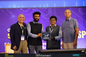
- Best Research Poster 2025 @ IDSPS Conference, New Delhi
- Best Research Poster Award: Issued by ISPEC 2025 organizing committee.
- AWSAR Award 2021: Issued by the Department of Science and Technology, Govt. of India for “disseminating the research outputs of Ph.D. among the masses in an easy to understand and interesting format to a common man”
- Institute Research Award 2021: Issued by IIT Madras as a “recognition of the quality and quantity of research during Ph.D.”.
- Prime Minister’s Research Fellowship 2019: Issued by the Ministry of Education, Govt. of India; The flagship Ph.D. fellowship that “seeks to attract the country’s best talent into research”.
- Best Major Project Award 2017: Issued by NIT Calicut as a “recognition of the quality and quantity of work done as a part of B.Tech project”.
Administrative Responsibilities @ IIT Bhubaneswar
- UG Coordinator of Department of ECE Oct. 2024-Present.
- Professor in Charge (IDEA Lab) July 2024 – Present
- Professor in Charge (Micro Fabrication and Characterization Lab) May 2024 – Present
- Faculty Coordinator for Placements and Internships (ECE) May 2024 – Jul 2026
- SES Aesthetics Committee Member May 2024 – Present